- Products
Fluorescence Spectrometer
Modular Raman Spectrometer
Finder 930 series Fully Automatic Raman Spectroscopy Analysis System Ultra-high performance scientific research CCD spectrograph High Performance Raman Spectrometer Confocal Raman System RTS-Mini Finder Insight Pro Raman Spectroscopy Handheld raman spectrometer Portable Raman Analyzer with Fiber Probe More>>Solar Cell System
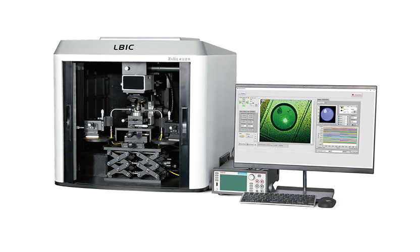
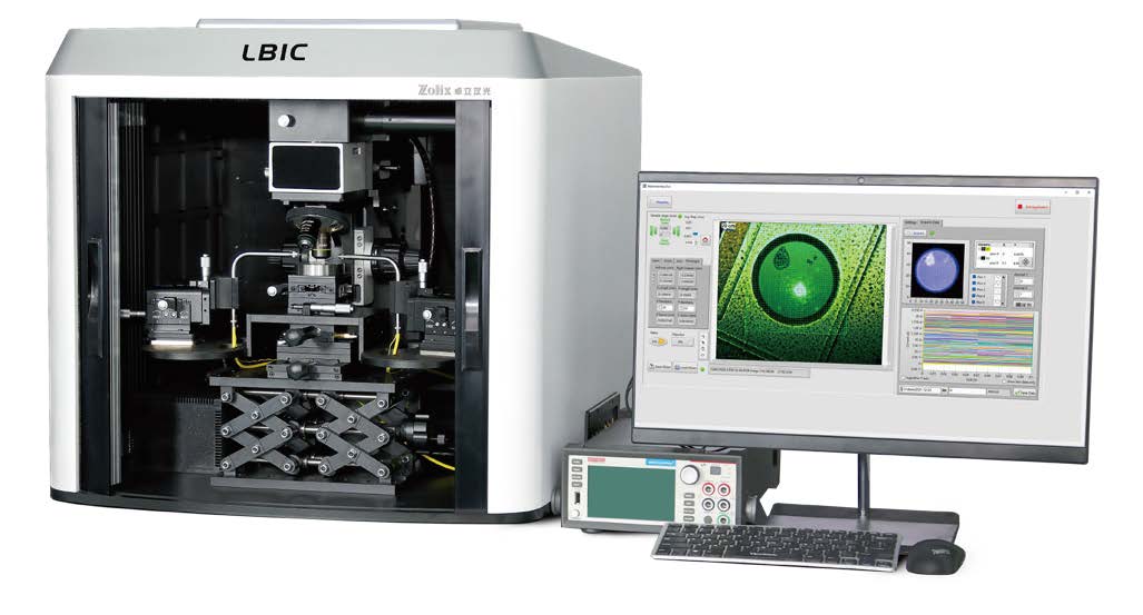
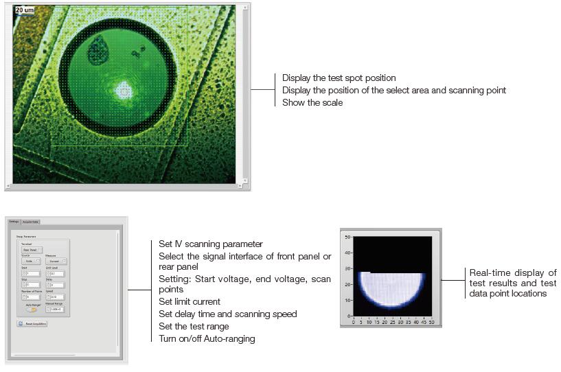
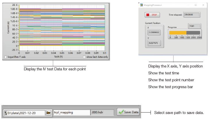
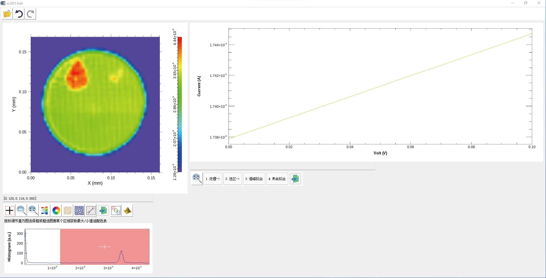
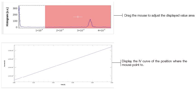
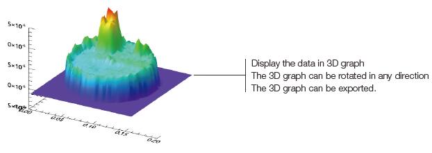
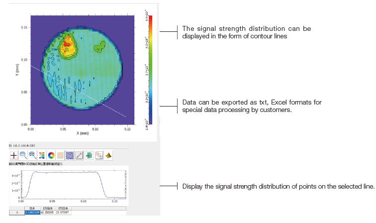
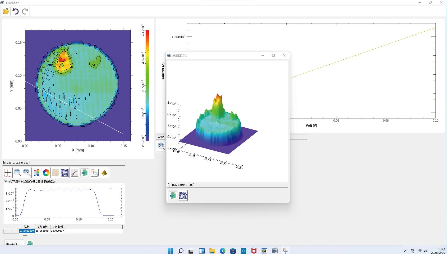
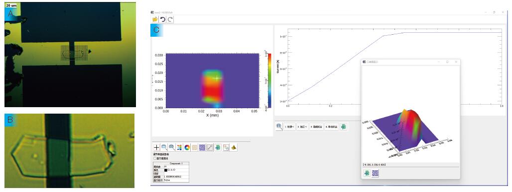
SolarIV series Solar Cell Voltage and Current(IV)Characteristics Test System Sirius series Solar Simulator QE-B1 Calibrated Monocrystalline Silicon Cell SCS600 Solar Cell Quantum Efficiency Measurement System SCS600-MAX Large Area Solar Measurement System DSR600 Photodetector Spectral Response Measurement System DSR300 Micro-nano Device Spectral Response Measurement System More>>Spectrograph & Monochromator
Motion Control
Motorized Linear Stages Motorized Vertical Stages Motorized Goniometer Stages Motion Controllers 2D- or 3D motorized alignment stages Multi-axis systems Piezo-Motion Units More >>Manual Positioners
- Applications
- Resources
- Services
- News
- Company
-
 13910278534
 010-56370168