CN
Home > Products > Solar Cell System > SCS600-MAX Large Area Solar Measurement System

SCS600-MAX

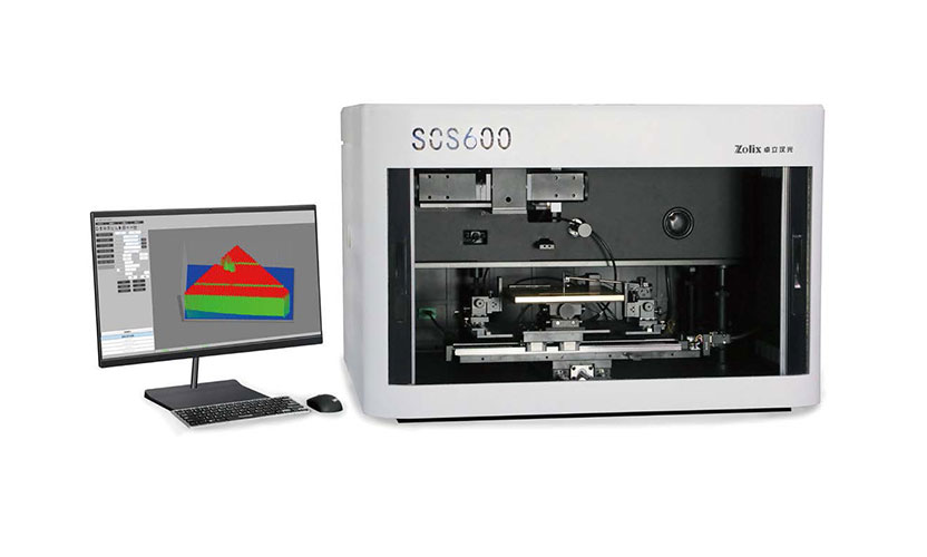
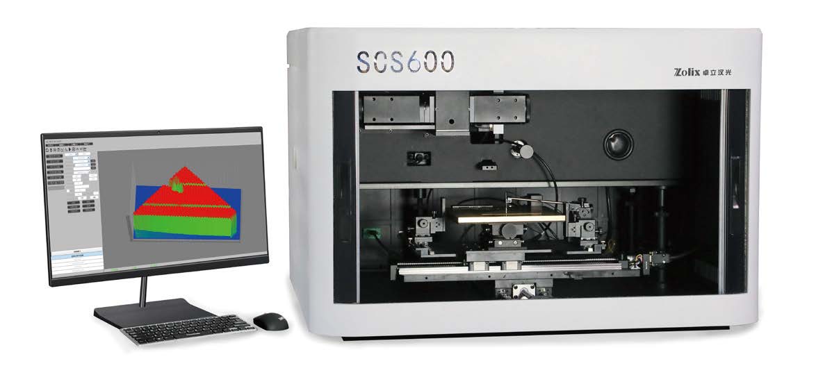
SCS600-MAX Large Area Solar Measurement System

Inquiry
Download
Details
SCS600-MAX Large Area Solar Measurement System
Functions
■ Suitable Cells: Large sized solar cell
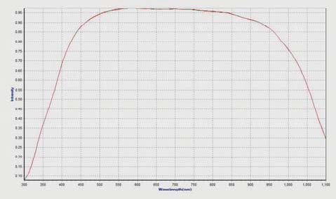
■ Spectral Range: 300-1100 nm, expanded to 1700 nm
■ Spectral responsivity, external quantum efficiency, photonelectron conversion efficiency, internal quantum efficiency,
reflectivity, transmittance, integral short-circuit current density, beam-induced current, quantum efficiency mapping, reflectivity mapping, beam-induced current mapping
■ Maximum Sample Size: 250 × 250 mm
■ Data Collection Mode: AC and DC test method
Features:
Full spectrum sunlight simulation, dual light source switching optional, high light intensity stability
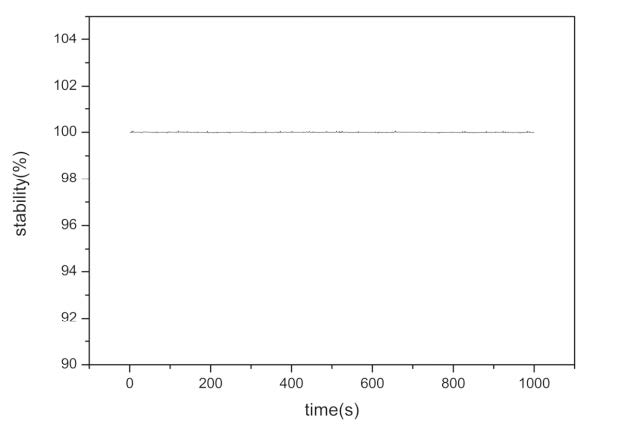
The system uses a dual light source configuration that complies with the latest IEC60904 standard, using xenon and tungsten lamps to cover the entire range of the solar spectrum. The light source features ultra-high light intensity stability, thus ensuring the high repeatability of the system test results.
1000s light intensity stability curve and change curve Test light source: dual light source, test time: 1000s, intensity instability <0.8%
High repeatability
Full spectral range repeatability test, testing frequency:
5 times, time interval: 1 hour.

User-friendly software

The software is an user-friendly software for complete instrument control and data handling on the SCS600-MAX system. It is used for generating quantum efficiency curve and photon-electron conversion efficiency, and so on.

The operation parameter settings can be saved as an independent configuration file and exported according to different samples, so as to realize the rapid restoration and testing. The raw data supports data export in various formats such as txt, excel, and pictures. It is very convenient to do the data processing and analysis.

Fast Mapping function
1) QE Mapping
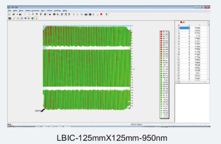
2) LBIC Mapping.
This function is mainly for large size cell, the maximum size is 250x250 mm.
The user could obtain the minority carrier diffusion length and defect distribution information.

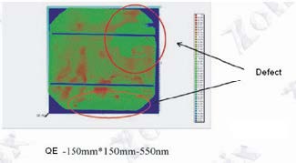
The up picture shows the result of IQE mapping of a 6" monocrystaline silicon photocell. In the top right corner is an area of the cell of much lower IQE. Such a defect is clearly visible in the mapped result but impossible to detect using normal visual techniques.

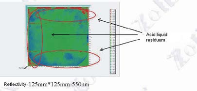
The up picture shows the reflectivity map from the same monocrystaline silicon cell The picture demonstrates that the cell has significant non-uniformity. The reason is due to residual acid left on the cell.


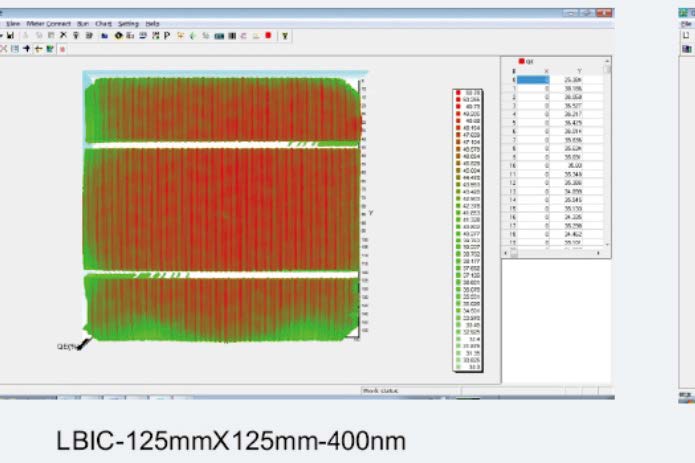
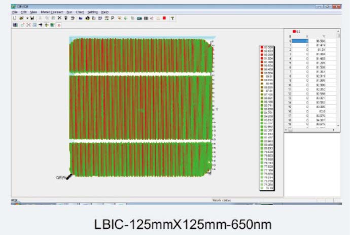
The above three Mapping data images are obtained from the one cell at 400 nm, 650 nm and 950 nm wavelength by scanning QE (LBIC). For the 650 nm and 950 nm maps, the QE data shows that the cell uniformity is better than at 400 nm. For the 400 nm data, the sample uniformity is obviously bad around the edge. By using different wavelengths of light the user can prove different incident depths within the silicon cell. The longer the incident light wavelength the further into the silicon cell the light will penetrate thus allowing depth profiling and examination of the inner depths of cells.

Configuration:
■ Light Source: 150W Xenon Lamp
■ Spectral Range: 300-1100nm, 1700 nm is optional
■ Light Spot Diameter: 2-15 mm
■ Monochromatic Light Band Width: < 10 nm
■ Step: 5 nm
■ Maximum Scan Area: 250 × 150 mm
■ Position Accuracy: 10 um